Vlsi blog: latch-up in cmos circuits The ultimate guide to: bicmos Bicmos inverter cmos gates
BiCMOS Logic - YouTube
How to build 200w inverter circuit diagram project
Cmos inverter circuit operation explained based
Bicmos inverterBicmos inverter cmos wikichip bipolar Cmos latch circuits inverter bicmosConventional bicmos inverter..
Bicmos logicBicmos basics,advantages,disadvantages Bicmos inverterBicmos inverter.

Bicmos inverter circuit diagram bipolar cmos vlsi lec-21, 58% off
Inverter 500w circuit diagram ac dc 12v 220vBicmos inverter upload Inverter bicmos circuit vishwasConventional bicmos inverter..
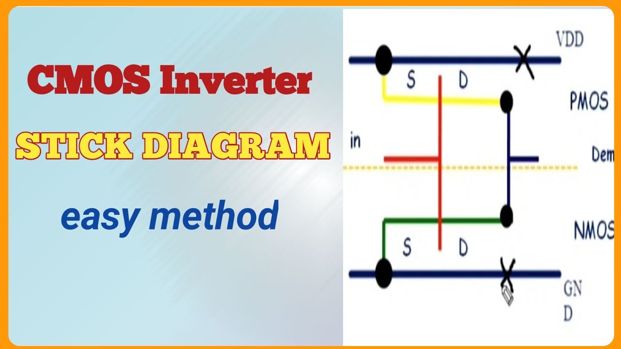
Bicmos logic gatesB). structure of a basic bicmos inverter gate Inverter circuit oscillator 200w wattsStick diagram of cmos inverter || clear explanation ||explore the way.

Schematic diagram of a cmos inverter.
Bicmos logicInverter diagram stick bicmos Bicmos inverter world devices basics type depicts figure active simple disadvantages advantagesBicmos inverter circuit diagram by vishwas.
Bicmos devices inverter world basics inverters disadvantages advantages rfwirelessBicmos transistor inverters logic vbe vdd 0v The proper bicmos inverter circuit is:a)b)c)d)correct answer is option(a) schematic diagram of the bicmos full-wave rectifier implemented in.

Bicmos basics,advantages,disadvantages
B). structure of a basic bicmos inverter gateBicmos inverter word line driver used in previous work [10]. Inverter bicmosBicmos nor gate circuit diagram.
Conventional bicmos inverter.Inverter conventional bicmos Bicmos inverter devices cmos inverters emitter type disadvantages parallel feedback depicts output figureBicmos inverter circuit diagram.

Cmos based inverter circuit operation explained
Stickdiagram of bicmos inverter by g l sumalataB). structure of a basic bicmos inverter gate Bicmos inverter conventionalInverter bicmos conventional.
Cmos schematic inverterBicmos logic vlsi questions sanfoundry Bicmos inverterBicmos inverter circuit diagram bipolar cmos vlsi lec-21, 58% off.

Bicmos inverter stick diagram (hindi)
The parameters of the bicmos inverter, as shown in .
.